In Part I of this series we described how to take an existing KiCad open source repository, fork it, and start making updates to customize the PCB.
This PCB will be ultimately sent to fabrication using our trusted service of JLCPCB using their PCB Assembly service.
My mission in this PCB project is to make a PCB where I can make User Interfaces using this display and LVGL. PCB purist will scream seeing that instead of making a whole new PCB I’m just modifying an existing one. That might be the longer road but here I don’t want to reinvent the wheel, being epdiy v7 working, I just want to extend the same PCB to add touch and connectors in the right place. Basically I wanted to pass from working like this
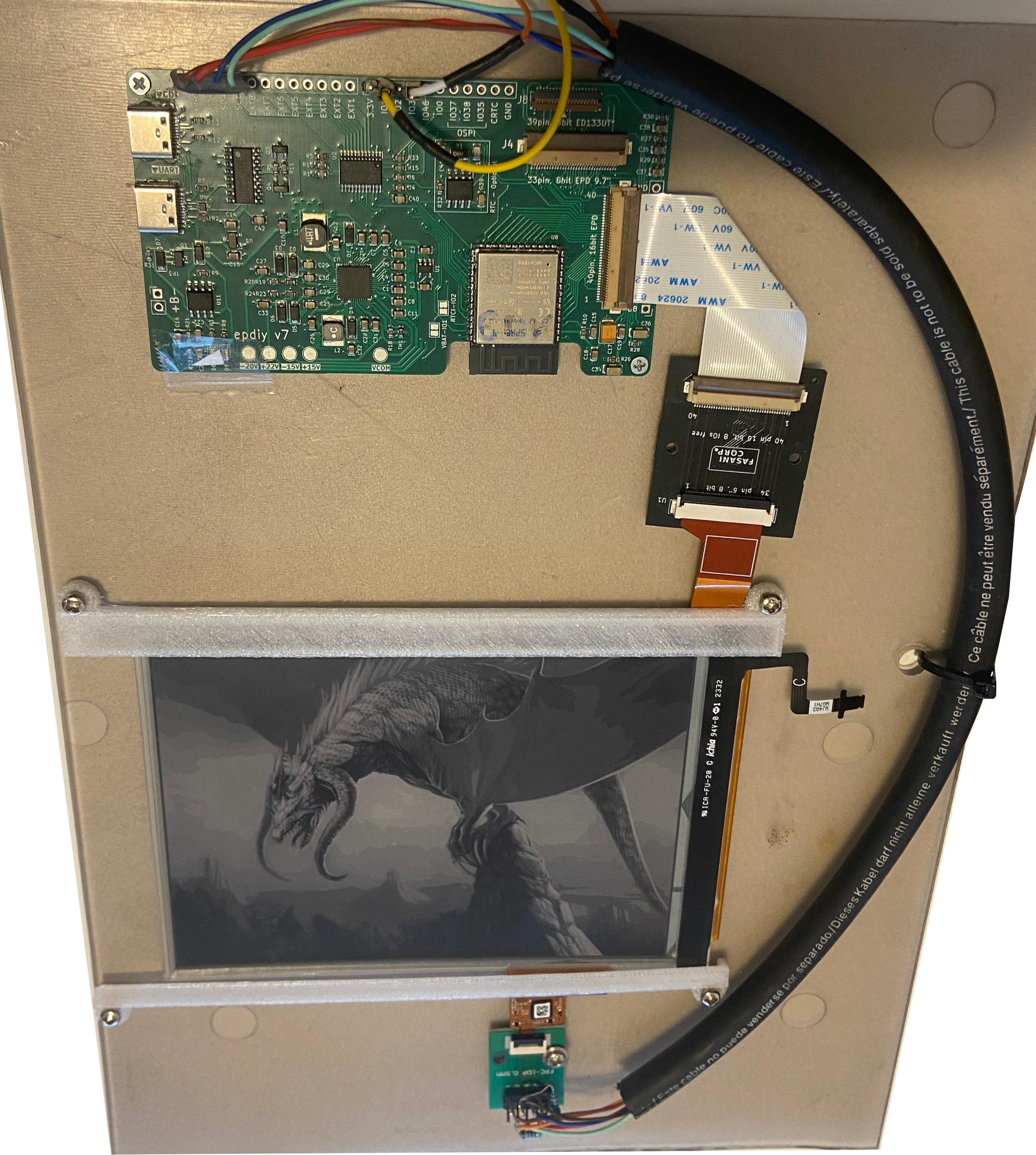
Uncomfortable and with FPC cables all over, what I really wanted, is to have a solid PCB where at least the 34 pins display connector and 8 pin touch connect to the board in the bottom. That is the primary objective here and not to make the perfect PCB to sell in Tindie :P
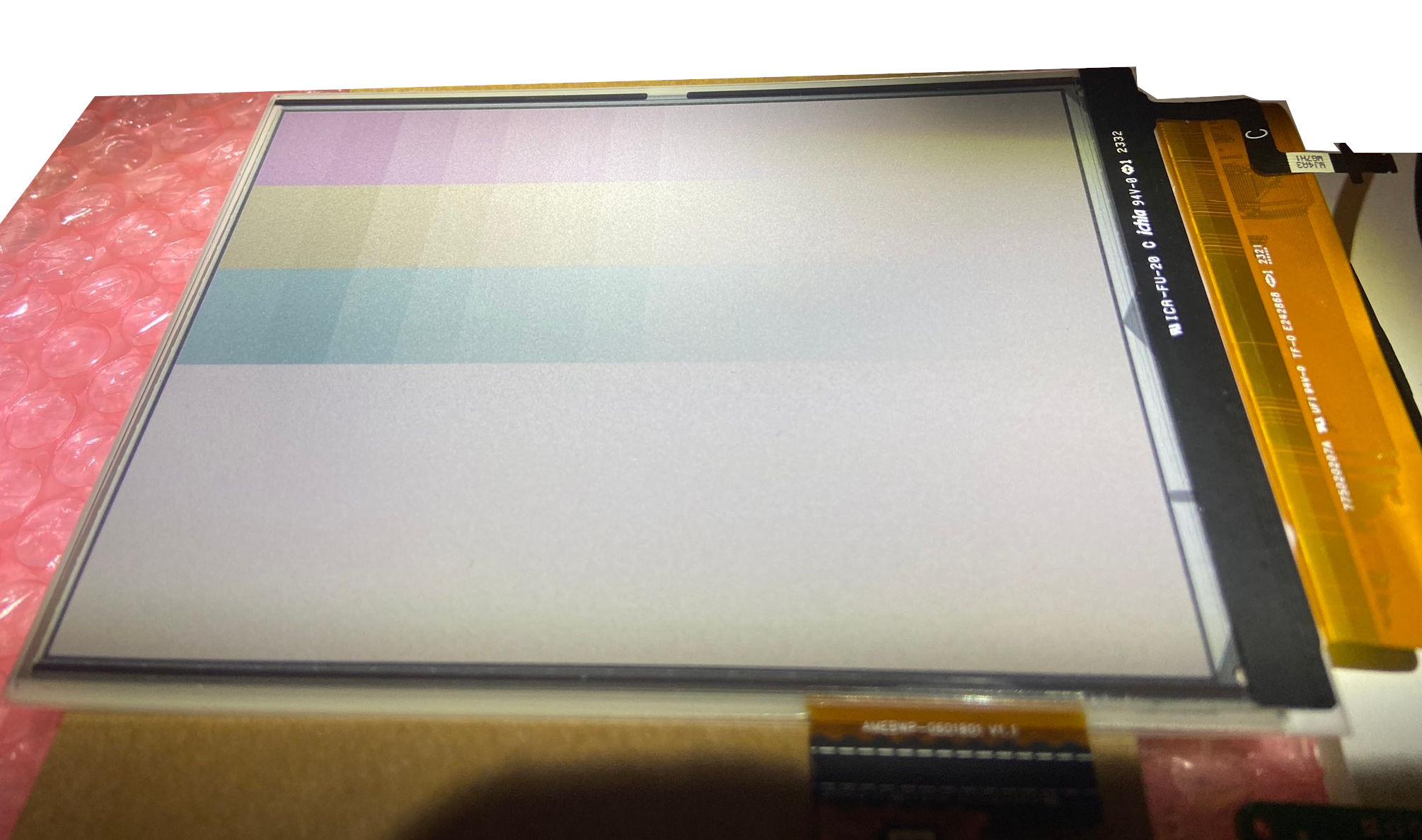
The main idea then is to prototype fast and have in the least possible time a working sample to keep on with the work of adding this display in LVGL and make it possible to make UX using C or C++. As you can see this display has a color filter over every pixel. So it’s colorful. Being a project collaborator already started working in adding color support to the epdiy component.

This is how it works after cleaning up non used D8 to D17 pins (Only used in 16 bit displays) and placing the 34 pins where it will be according to my technical drawing prototypes described in Part I.
This is how it works after cleaning up non used D8 to D17 pins (Only used in 16 bit displays) and placing the 34 pins where it will be according to my technical drawing prototypes described in Part I.
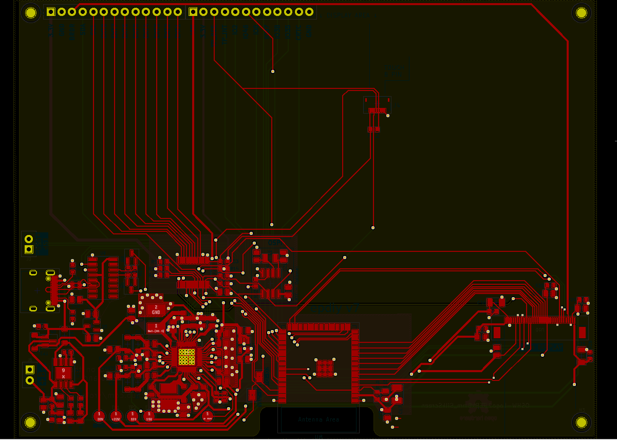
Ninety minutes later and after some more extensive cleaning the display is starting to be connected. Needs many checks still to get validated and DRC checks to ensure the things are well done and all is connected like it should.
At this point I also placed the touch FPC connector in the right place again taking as a reference the design measurements taken in first part of this blog series. This placements are going to be double checked exporting the PCB in 3D and printing those 2 FPC connectors. That’s a nice feature that KiCad PCB new has: It let’s you export the PCB in Step or WRL that you can convert to STL and 3D-print importing that in any Slicer software.
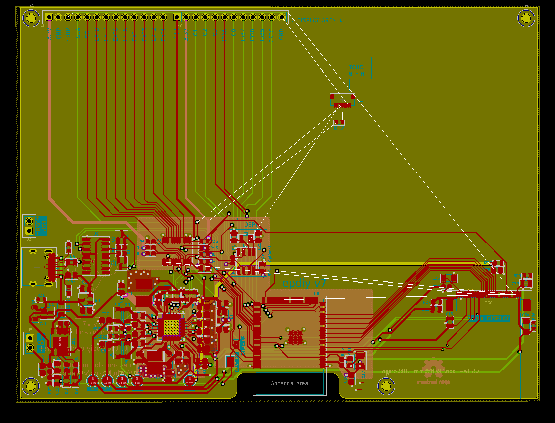
Also since we are going to place and connect the Touch, let’s then take the IO decisions so it’s already connected to the MCU:
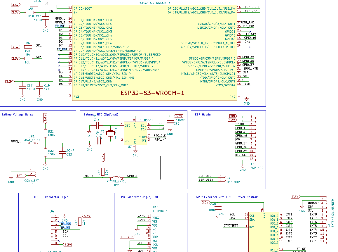
I choose then IO3 for the TP_INT that goes low when it detects a Touch interaction and IO9 for RST that is usually pulled down when initializing the touch IC. Then it comes the manual work of validating everything first with the eyes and clear thinking. And doing the routing.
I’m not good at it. I learnt this by doing and looking how other people that is certainly much better than me do it in different projects. Routing for me can be defined as the shortest logical way to connect A to B, but taking in account that are many signals going to one FPC connector and they all have to arrive to destination having the minimal possible hops (VIAS) to another layers. That is a rule at least for the Parallel data transmission pins, you don’t want to have 4 hops in one of those, sending the parallel super fast data transmission through many layers. But sometimes things are not easy or straightforward enough to make things as you want and sacrifices should be made.
There 2 layers in this 4 layers PCB that are the most important:
1. F-cu Front one is where most signals go and also has some GND panes
2. B-cu is the back one where all other signals are routed and also the high voltages of the display go
My strategy is then follow what the original author of the PCB did and try not to route any other trace in the interior Sandwich layers (In1 -> GND pane, In2 -> 3.3 V mini pane)
As an important remark this displays need some Capacitors for the high voltage lines where the datasheet specifies that need to be as close as possible to the display. Then we place that close to the FPC connector or in a central point if you have multiple connectors like in epdiy v7 board.

Back copper layer: Other signals that won’t pass through front and also high voltage lines
Now let’s make a zoom in the display connector to check some details:
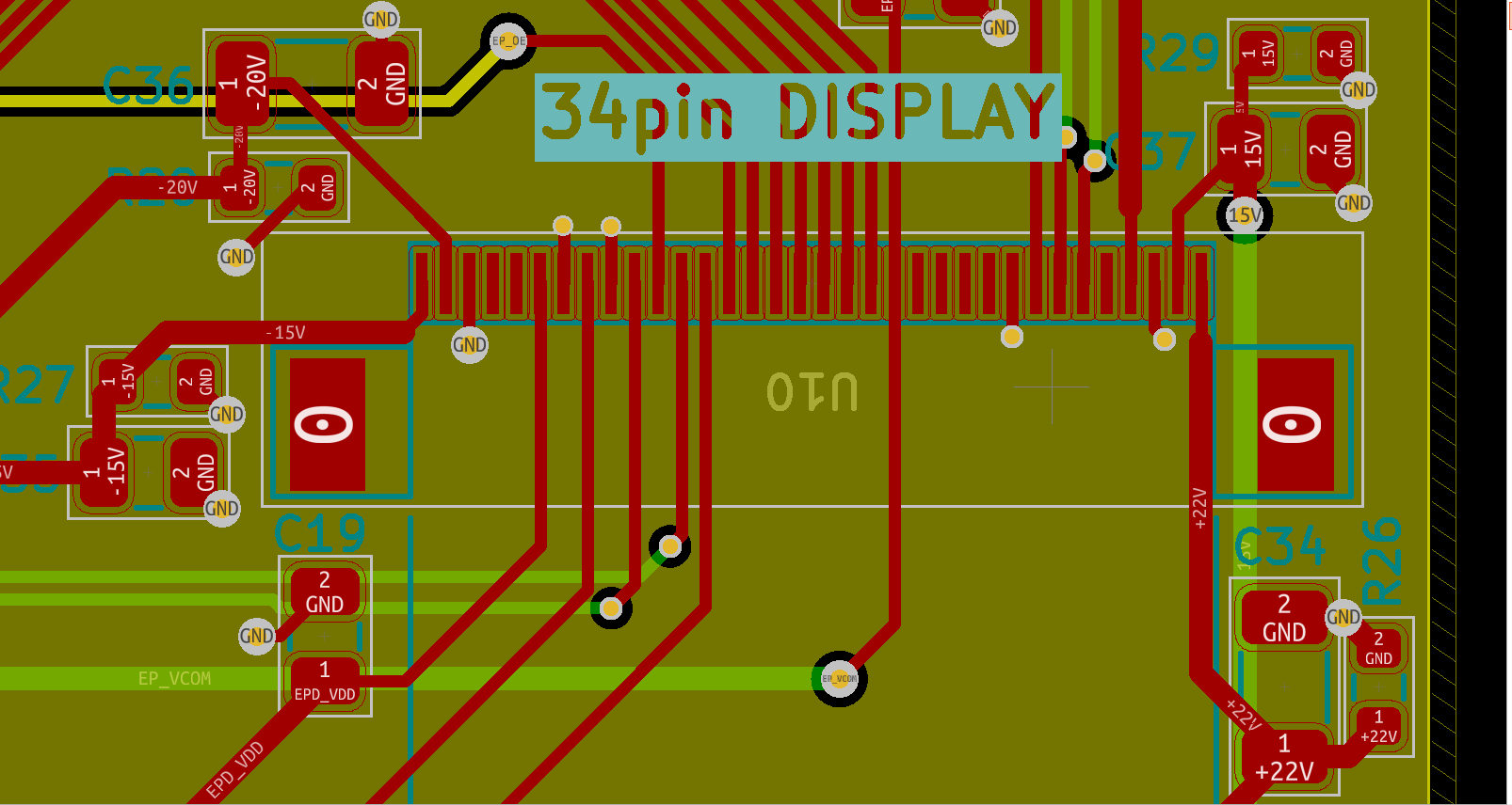
You can see here that the load capacitors are close to the FPC, the data signals on TOP of U10 have no hops, and also the VCOM and other voltage traces are bigger. Because they are rather long and don’t want to make them super thin so they loose the minimal voltage on the way. Also we will put a very descriptive level saying loud how many pins has the FPC connector and mentioning clearly that is for the display.
Keep tuned, part III will come very soon!
If you like our work and publications there is a chance you like our PCB products. Please visit our Tindie store and check if there is something that can inspire you for your next projects.

One response to “Making an epdiy v7 Kaleido clone – Routing – part II”
[…] this is already taking shape!Keep tuned, part II is being written while you pass the […]