In this post we are going to clone the epdiy v7 Hardware repository and make a custom version to control a Eink Kaleido 6 inches display.
The existing epdiy v7 can control this epaper already but we want to make a PCB clone specifically for this display, removing other connectors and adding additional ones for Touch and Front led lights (FL)

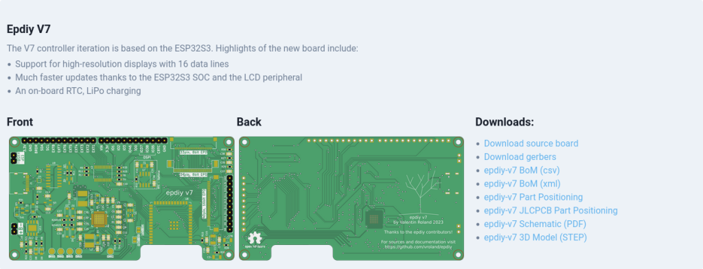
Existing epdiy v7 PCB looks like this in the latest version

The first thing we will do is to identify and make a technical drawing of the display FPC connectors since we need to place those precisely on the PCB. We measure the existing 4 layers PCB with the Calliper giving a thickness of 1.6 mm. Taking the display measures too:

We will 3D-print or find a piece of cartoon that is this exact width. The idea is to comb those cables and draw them, so we can replicate this in our PCB design:

As you can see what we did is to draw how the FPC ribbon cables will look like if we comb it over the PCB, 3D-printing a PCB simulation with the exact size. Also we can see that the FL cable of the Kaleido version we have is a bit different than the latest version, so we will try to add 2 different connectors to cover both display versions.
Now we will start the process of cloning existing epdiy v7 PCB in order to start making our own custom version.
Epdiy hardware repository address: https://github.com/vroland/epdiy-hardware
We will sign in with our Github account and use the Fork feature. What it does is to fork, or clone, this repository in our own Github making a copy of the latest master branch. This is a very useful feature since also enables open source collaboration. Having a fork of the original repository, enables you to make a new feature in a PCB or any library, and make a “Pull request” to the original repository signaling the author that you want to get your changes reviewed and possibly merged back, effectively collaborating in the project.
But in this case we are doing this for ourselves, just for the sake of creating a new controller, that will be for the moment hosted in our github repository and open to the world. After forking, for me is important to update the name, to reflect what you are doing. So I will call my fork epdiy-hardware-versions and also update the description to:
This fork will contribute adding additional board versions, like Kaleido w/touch, SOC only version, etc
This important because otherwise every repository may have hundreds of forks with the same name and when you search for something you struggle to find out what was the Fork idea and what new feature it brings!
Now we have a fork of the original repository with our custom name and description, let’s clone it locally and put our hands at work.
After doing that in order to make things more coherent all over, I will also rename all Kicad Files: .kicad_* (sym, sch, pcb, etc) to the new name:
For that you navigate to your new repository in Github and you can see a Green button called: <> Code
This button offers an URL that you can copy and then clone locally.
We will then open the command line and clone it in our Documents folder (Or wherever you desire)
git clone https://github.com/martinberlin/epdiy-hardware-versions.git –recursive
I’m adding –recursive since this repository has submodules, meaning that has linked additional repositories inside, for example to fetch certain KiCad library components like TP4056 or other modules. If you don’t clone recursively it will fetch only the main repository.
After doing this then we already have a local copy of all necessary KiCad source files. Let’s then copy the full directory epdiy-v7 that has the latest version of the PCB and place it in a new folder that we will call: versions/v7-kaleido-34
Just to signalize that this is a Kaleido 34 pin parallel Eink controller PCB.

Awesome! At this point we already can open v7-kaleido.kicad_pro and start working.
First we will handle the Schematics. We will remove connectors we will not use and add the ones that will be handled in this PCB.

One important part of JLCPCB is “My parts” library. JLCPCB let’s you pre-order parts and keep them there in your Parts Lib, so the components can be used for the PCBA or PCB Assembly process. This way you can buy in larger quantities in case you need to produce many PCBs and most importantly you can keep there components that are scarce and that their price might change affecting your production. For example for this particular PCB, the PMIC or power Mic that generates the display needed voltages (+15 / -15 / +22 etc) is the Texas Instruments TPS65185. This is not always available so I make sure to have always at least 50 units in my Parts lib, ensuring that if they get out of stock I can still produce 50 PCBs more. And this way you can keep many components “in your stock” since every time one component is out, you need to loose precious time in your new order, re-adapting your BOM, maybe placement files if they have a different footprint, just because this particular component is not available anymore. Believe me I lost many hours on this until I learnt the simple lesson to keep all essential stuff in “My parts lib”.
Adding the new FPC connectors
Let’s add those to the schematic. According to the Datasheet the type of connectors are:
Recommended Connector Type of Front Light (FL)
FH34SRJ-6S-0.5SH(50)
Touch Panel
FH34SRJ-8S-0.5SH(50)
We also need to check if the FPC needs to have bottom contacts or top. In our case and after making our technical drawing we see is bottom connection (Double check this always!) Both connectors are very similar, both 0.5 mm pitch, only that Touch Panel has 2 pins more than the FL one.
In this example we are going to focus only on the Touch Panel and we will leave the FL one for next part of this series, since I would like to make an additional boost circuit for that, since I don’t want to use TPS65185 to generate the Front Leds power.
We will open then https://jlcpcb.com/parts and search directly for FH34SRJ-8S-0.5SH. It’s not always that straight-forward but this time we’ve found the exact part:

In that image we can see that is on stock. And there is a nice amount. But for example if there would be only 100 in stock and I still need some weeks to finish my design, then I will order 50 more to My Parts Lib. Then you can see that instead of 11 cents, I will pay 9 cents per 50 units, already reducing the price of the PCB. That is not big, but multiply that for many parts, in bigger quantities and you can see how the end price changes.
Let’s now fish for the Footprint and if it’s available the 3D .step file, so we can preview our PCB.
For that there are a couple of nice websites but I use mostly 2:
https://componentsearchengine.com
https://www.ultralibrarian.com both need you to register in order to download Files.
Good luck with the 8 pins Hirose connector, the 3D seems to be available and the footprint is available in UltraLibrarian:

Note: Usually for this I don’t use a custom symbol since it exist already 8 pin options. So I download only footprint and 3D-Model. But you can do it your way, I just want to go as fast as possible, without caring of the “only visual” details.
We will download the ZIPs and copy them to the 3dmodel and footprints.pretty Folders.
I renamed in the Preferences -> Manage Footprint libraries (KiCad)
The library epaper-breakout to the more generic name “footprint” since I will like to search in that folder for all my new footprints. In order to make that complete I also need to rename existing TPS65185 in the schematic to this new name. To add the new Symbol I will search for Connector -> Conn_01x08_Pin (generic socket connector)
And before assigning the connections will check the panel datasheet for the Touch pin-out:
Pin Signal
1 GND
2 NC-No Connection
3 XRES – optional pullup 10K
4 INT 10K pullup
5 SDA (I2C)
6 SCL (I2C)
7 NC
8 𝑉𝐷𝐷 _TP 3V3 Power supply
In our new symbol the Conn_01x08_Pin we will click on Properties and select our footprint, that we copied in the footprints.pretty folder from UltraLibrarian:
footprint:CONN8_FH34SRJ_HIR
This will enable us after cleaning the components we don’t use, to resync the schematic, and get the new footprint already placed in PCBnew.
Now we will open PCBnew and remove the connectors we already deleted in the Schematic, the 33 pin (9.7″) and 39 pin (13″) FPC connector.
And we start the re-dimensioning process to adapt our PCB to the new panel, going back to the original technical drawing we made at the beginning, for this is useful to select only the Edge.Cuts layer and Toggle the other layers inactive like this:

Nice this is already taking shape!
Keep tuned, part II is being written while you pass the page…
If you like our work and publications there is a chance you like our PCB products. Please visit our Tindie store and check if there is something that can inspire you for your next projects.

One response to “Making a epdiy v7 Kaleido clone – part I”
MINOR UPDATE: Because we copied a Kicad project repository that has submodule Footprints you might get errors when you open the Footprint editor.
That is easily solvable either making Symlinks to the location of the footprint or simply opening the Preferences -> Manage Footprint Libraries and correcting the paths so KiCad finds them