Cinwrite SPI HAT for IT8951 parallel epaper controllers
This new Cinwrite SPI Master ESP32S3 PCB goal is to provide:

- ESP32S3 Espressif MCU with 2MB of external RAM
- WiFi
- BLE
- DS3231 real time clock and small CR1220 coin battery to keep time
- Fast 40Mhz SPI
- 3V to 5V step-up (And a way to enable this boost converter)
- 3.7v LiPo battery charger
This Cinwrite PCB is open source Hardware that you can explore and even adapt to your needs.
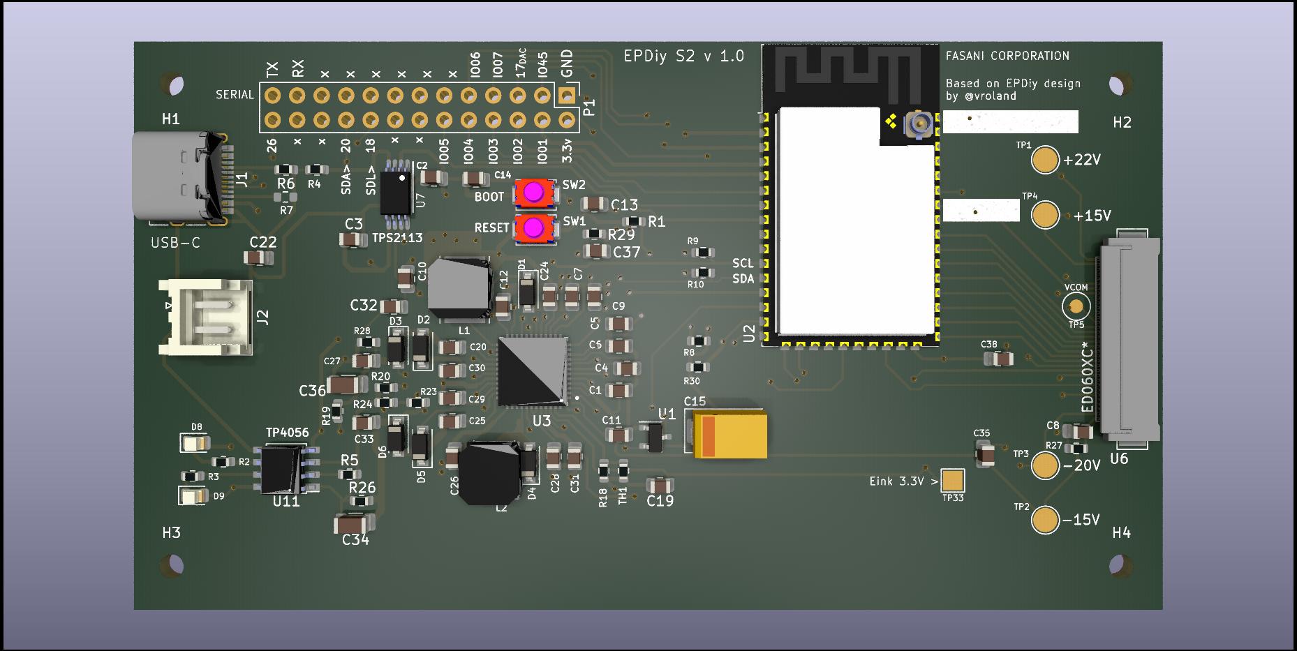
2022/ EPDiy ESP32-S2 Prototype V1.1
Still a working progress, this 8 data lines controller for Kindle-like epaper displays, is the main project for 2022. The design is based on original epdiy V6 PCB a project by @vroland. What is changed in this version is that it does not use PCA9555 port expander and also takes profit of the S2 feature of direct firmware updates using the USB port. This version aims to use a slightly bigger PMIC (7mm that has a 0.5 mm pitch) albeit will support only displays that consume up to 130 mA. Also the software needs to change since we ditched out the GPIO expander with the aim to have a simpler and cheaper PCB. – Prototype was cancelled since we want to use S3
Wasted 200€ in production costs, but learnt a good lesson, which will make next prototypes much more cost-effective.
2021/ ESP32 Tinypico HAT for UC8156 epaper displays
This was actually my introduction to KiCad after seeing some good video tutorials and get more acquainted about hardware hacking and electronic design. I had at home 3 epaper displays since I programed time ago a C++ class to drive them with my ESP-IDF component Cale-idf.
The 1.1″ Lectum display from PlasticLogic is a flexible active-matrix EPD with Ultrachip UC8156 single chip EPD controller, integrated drivers and power management. The technology of this epapers is very modern and they refresh super fast this one taking less than half a second. They also support 3 levels of gray plus white and partial refresh. Here you can find more technical documentation about this epaper displays (cale-idf Wiki)
This is my first PCB design that is on sale in my Tindie store.
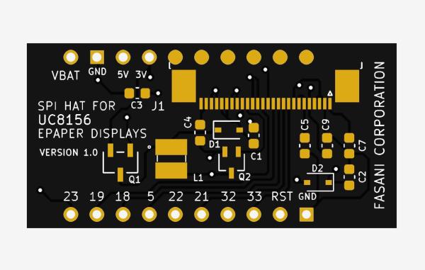
Tinypico ESP32 connections for the UC8156 SPI adapter:

SPI_MOSI=23
SPI_MISO=19
SPI_CLK=18
SPI_CS=5
RST=21      * 21 is SDA (As default in ESP32)
BUSY=33

*Note: In V1.0 the RST pin is using IO21. On next revision I will change this to use IO32, so the default SDA pin is not used.
My design process using KiCAD
I’m not an electronic educated engineer. I know only basic circuits, the theory of Ohm and how capacitors, transistors and other components can work together. But the essential thing is that when I was 9 or 10 years old I already started to get acquainted with electronics since my father designed equipment for lights control (Discotheques) and later repaired Mc Donalds restaurants equipment. He used to design PCB’s when online sites like JLPCB did not existed, and you had to go personally with your sample to a place where someone will analyze your prototype and prepare a PCB for you. At that young age is when I started soldiering and learning the basics of electronics.
I like also technologies like TFT displays and epapers. On the PlasticLogic and Goodisplay epaper displays, usually the ones that use SPI for communication have a controller inside that already generate the high voltages they need. But the thin surfaces are not enough to place the needed coils and capacitors. To generate high voltages, in silicon, its hard and expensive to implement relatively large inductors and also capacitors so these parts are usually added as external components. That’s why you can see that this epaper HAT has this external “help” to the UC8156 driver inside, without that the high voltages that are usually +15 -15v or more, would not work and you would not see the Eink particles moving up/down.
My process is quite simple and straight-forward. First I check the requirements that this particular displays need, for example existing UC8156 controllers, and I ask for specifications.
Then I work on the schematics and check that every pin from the HAT goes to the expected IO or power line where is going to be mounted. After every change design rules checker (DRC) is applied and also I try to go over the lines with my mind, and try to see if the overall thing makes sense.
Usually after the schematics are done and everything works at least in paper, then I usually consult with people that know 20 times more than me about electronics, to get wise advice. Only after this advice and implementing the proposed changes I export the Netlist from the Schematic and start building the PCB design program of KiCAD.
If I’m building a HAT usually the best is to check if the board designer where this HAT will be placed can help, in case of tinypico.com is Unexpected Maker, can give me a base design to import in KiCAD. Or at least the base footprint so I get the precise pin location to design on top. In this case Seon was nice enough to give me access to this, so I started with the right base.
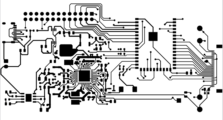
And then it’s the time to import the Netlist that brings all the components placed in the Schematic together. This is the moment of the big mess, where all pins are connected with lines, generating something that is called “Rats nest”.
Usually for simpler designs like the HAT you can see above I use a 2 layer PCB since it’s enough. And that’s where starts the placing elements, trying that this lines cross as least as possible. There is no perfect design. There is an optimal design that I think it can work for the use-cases I’m targeting.
After this comes the moment to place the small tracks and Vias in case you need to go to the down layer. It’s important to notice that in JLPCB microVias are not supported. So independently of the number of layers you select, a hole will go through all of them. Even if microVias would be supported is a super expensive technology that only a few can do.
After hours of routing, taking care that the power lines are a bit bigger than the signal data lines, and many rounds of Design rules checking then you might have the first 1.0 version of your prototype.
My personal checklist:
- Make a list of what IOs need to be pulled up in your design (Ex. I2C data lines need to have pull-ups to 3.3v in ESP32)
- Same list of IOs that need to be pulled down
- Re-read the Datasheets of the components and make sure you are respecting what is specified there (Specially if implementing something from the first time). Many times you will need to repeat your design, spending precious time and money, just because you are sure that the design is right and you will bite the dust. Specially power management chips and alike, need special conditions in turn to generate voltages, etc. You miss one thing in the design and most probably it won’t start.
- KiCAD has a nice Gerbers Viewer, that I initially though was only for experts, but examining the raw layers that you actually send to fabrication is a really good idea. Print your layers in a A4 page (extend it to size) and check if everything makes sense. Checking your layers one by one is an interesting view, that you usually don’t get on PCB new.
- Make sure that the PCB size is what you are expecting for and that it has proper mounting holes if you are going to make a case for it (For example a 3D-printed case, also possible to order in JLPCB)
Many other checks would be needed. Consulting with other peers is always a good idea before sending something to fabrication. Because other people might see obvious points, that you the proud owner of the design, cannot discover. So be humble is asking for a review, since we all make mistakes and making many revisions of a prototype can be expensive. After this peer review you can be ready to export the fabrication files (Gerbers/ Drills for the VIAs) and the pick and place SMD components that you can use if you wish to have this commodity done for you.
I advice to order at least for 10 or 15 PCBs since making 5, most of the components have a minimum requirement of 15 and you will not get the not placed components. So it’s a good balance to ask for at least 10 PCB’s with SMD mounting.
Visit also our blog friends:
