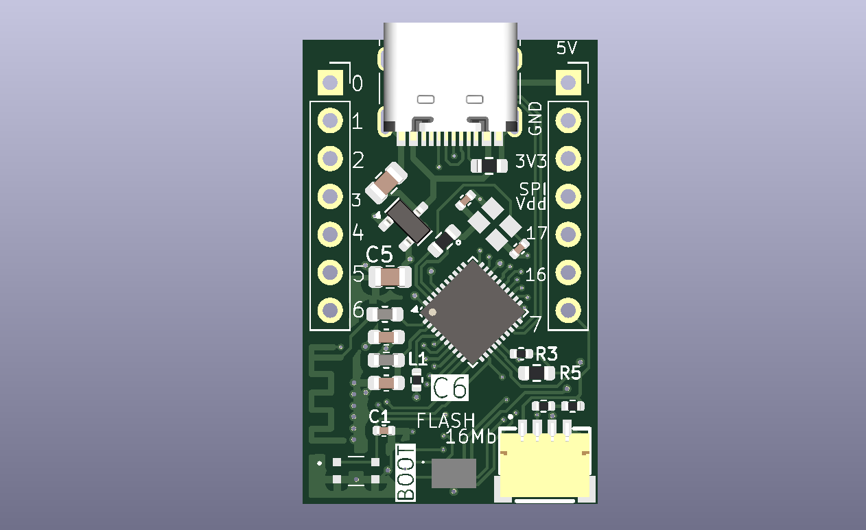
In last board we send to fabrication the C6 ULP project I’ve failed miserably. Why?
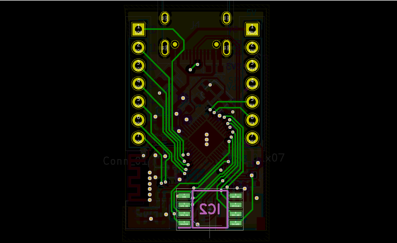
The board routing and schematics was Ok! But I’ve wrongly mistaken the ESP32C6 MCU using a 40 pin QFN that does not come with built in flash.
You can find the open source KiCad files in this repository.
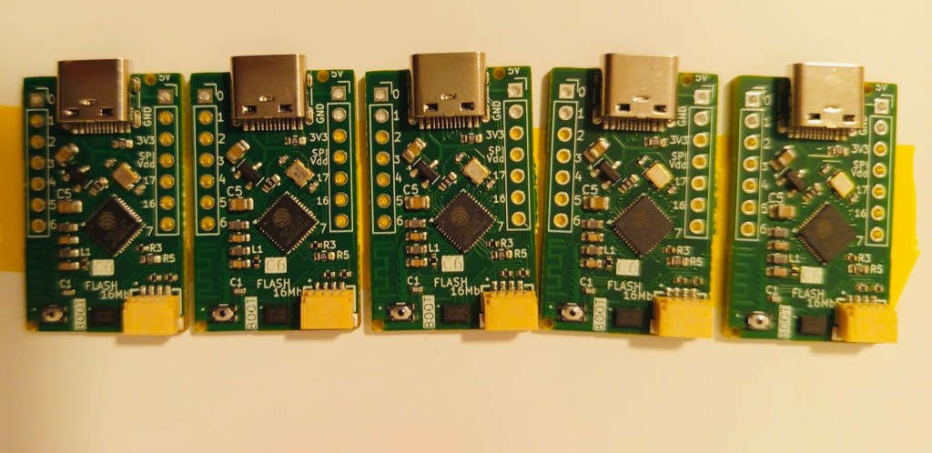
Sadly that is the bad kind of mistake. Because if it does not have flash then you cannot store your program anywhere rendering the PCB as a bricked device that you cannot flash. Then I’ve had two options: To use the C6-H4 32 pin QFN that comes with 4Mb internal flash or to use an external flash IC. As I never did that I wanted to make a “cheap test” first which resulted in the following PCB that we sent to JLCPCB assembly:

It worked out right but I’ve learnt 3 important lessons in the process.
- Always try to go with the build in flash. The fabricant will for sure select the less power consumption IC and will use the best layout for it. Remember that layout is in some circuits very important. Specially for high speed data and any RF device. Flashing this device works but double slow than the built in flash and it’s using a flash IC with 16 Mb that is too big and probably consumes more than the built in C6 32 pin QFN
- Double check the datasheet to make sure that the MCU you selected for your project has built in Flash. If not, do not forget to add it externally!
If that is the case check the datasheet to get examples of the best layout and wire it trying to use short and precise routing with the least possible hops between layers. - If you want to use existing adapters, like the one we already have for Seeed XIAO, you can go for it. Usually you can find the footprint and documentation files in their website
So was it worth to spend 50 USD in 5 test PCBs?
In my opinion yes. Because at least we know that we are not going to use external Flash ICs even though they do work for the conclusions we got in this test.
And finally because we’ve 5 nice and good looking own XIAO MCUs that expose different pins. Where also we tried to do the first PCB Antenna design that seems to work and connect to WiFi. The RF design was done following this Texas Instruments application paper.
And then having your own XIAO design you can add whatever you want to it. For example battery charging that they don’t have. Or a QWIIC I2C connector. Whatever fits your next prototype can be added into the PCB.
We would like to thank JLC for supporting our ideas and projects!

Larry test with this device and a 128×128 1.3” Sharp LCD driving it using ULP had an average consumption of 19 uA (18.87 micro amper)
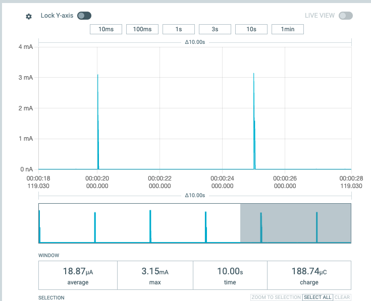
This power profile is of this PCB driving a Sharp 128×128 memory LCD and updating the display every 5 seconds (completely running within the ESP32-C6 ULP). 18.87uA average current from the 5V pin!
If you like our work and publications there is a chance you like our PCB products. Please visit our Tindie store and check if there is something that can inspire you for your next projects.
